- 您现在的位置:买卖IC网 > Sheet目录492 > NTP60N06LG (ON Semiconductor)MOSFET N-CH 60V 60A TO220AB
�� �
�
�NTP60N06L,� NTB60N06L�
�Power� MOSFET�
�60� Amps,� 60� Volts,�
�Logic� Level�
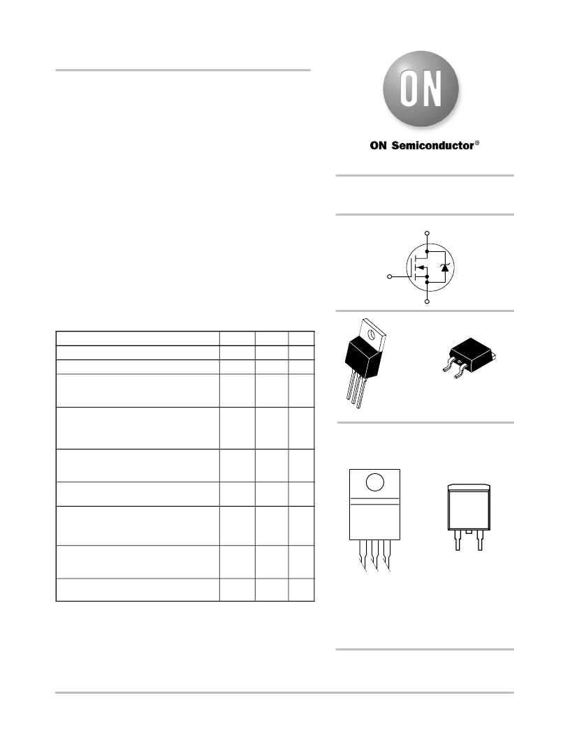
�N?Channel� TO?220� and� D� 2� PAK�
�http://onsemi.com�
�Designed� for� low� voltage,� high� speed� switching� applications� in�
�power� supplies,� converters,� power� motor� controls� and� bridge� circuits.�
�Features�
�?� Pb?Free� Packages� are� Available�
�60� AMPERES,� 60� VOLTS�
�R� DS(on)� =� 16� m� W�
�N?Channel�
�D�
�Typical� Applications�
�?�
�?�
�?�
�?�
�Power� Supplies�
�Converters�
�Power� Motor� Controls�
�Bridge� Circuits�
�G�
�S�
�MAXIMUM� RATINGS� (T� C� =� 25� °� C� unless� otherwise� noted)�
�4�
�Rating�
�Symbol�
�Value�
�Unit�
�Drain?to?Source� Voltage�
�V� DSS�
�60�
�Vdc�
�4�
�Drain?to?Gate� Voltage� (R� GS� =� 10� M� W� )�
�V� DGR�
�60�
�Vdc�
�1�
�2�
�D� 2� PAK�
�Gate?to?Source� Voltage�
�?� Continuous�
�?� Non?Repetitive� (t� p� v� 10� ms)�
�Drain� Current�
�?� Continuous� @� T� A� =� 25� °� C�
�?� Continuous� @� T� A� 100� °� C�
�?� Single� Pulse� (t� p� v� 10� m� s)�
�Total� Power� Dissipation� @� T� A� =� 25� °� C�
�Derate� above� 25� °� C�
�Total� Power� Dissipation� @� T� A� =� 25� °� C� (Note� 1)�
�V� GS�
�V� GS�
�I� D�
�I� D�
�I� DM�
�P� D�
�"� 15�
�"� 20�
�60�
�42.3�
�180�
�150�
�1.0�
�2.4�
�Vdc�
�Adc�
�Apk�
�W�
�W/� °� C�
�W�
�1�
�2�
�3�
�3�
�TO?220AB�
�CASE� 221A� CASE� 418B�
�STYLE� 5� STYLE� 2�
�MARKING� DIAGRAMS�
�&� PIN� ASSIGNMENTS�
�4�
�Drain�
�4�
�Drain�
�Operating� and� Storage� Temperature� Range�
�T� J� ,� T� stg�
�?55� to�
�175�
�°� C�
�NTx�
�Single� Pulse� Drain?to?Source� Avalanche�
�Energy� ?� Starting� T� J� =� 25� °� C�
�(V� DD� =� 75� Vdc,� V� GS� =� 5.0� Vdc,�
�E� AS�
�454�
�mJ�
�NTx60N06LG�
�AYWW�
�60N06LG�
�AYWW�
�L� =� 0.3� mH,� I� L� (pk)� =� 55� A,V� DS� =� 60� Vdc)�
�Thermal� Resistance,�
�?� Junction?to?Case�
�?� Junction?to?Ambient� (Note� 1)�
�Maximum� Lead� Temperature� for� Soldering�
�Purposes,� 1/8� ″� from� case� for� 10� seconds�
�R� q� JC�
�R� q� JA�
�T� L�
�1.0�
�62.5�
�260�
�°� C/W�
�°� C�
�1�
�Gate�
�2�
�Drain�
�NTx60N06L� =� Device� Code�
�3� 1� 2�
�Source� Gate� Drain�
�3�
�Source�
�Maximum� ratings� are� those� values� beyond� which� device� damage� can� occur.�
�Maximum� ratings� applied� to� the� device� are� individual� stress� limit� values� (not�
�normal� operating� conditions)� and� are� not� valid� simultaneously.� If� these� limits� are�
�exceeded,� device� functional� operation� is� not� implied,� damage� may� occur� and�
�reliability� may� be� affected.�
�1.� When� surface� mounted� to� an� FR4� board� using� the� minimum� recommended�
�x�
�A�
�Y�
�WW�
�G�
�=� B� or� P�
�=� Assembly� Location�
�=� Year�
�=� Work� Week�
�=� Pb?Free� Package�
�pad� size,� (Cu� Area� 0.412� in� 2� ).�
�ORDERING� INFORMATION�
�See� detailed� ordering� and� shipping� information� in� the� package�
�dimensions� section� on� page� 2� of� this� data� sheet.�
�?� Semiconductor� Components� Industries,� LLC,� 2005�
�August,� 2005� ?� Rev.� 3�
�1�
�Publication� Order� Number:�
�NTP60N06L/D�
�发布紧急采购,3分钟左右您将得到回复。
相关PDF资料
NTP65N02RG
MOSFET N-CH 25V 7.6A TO220AB
NTP75N03-006
MOSFET N-CH 30V 75A TO220AB
NTP75N03L09G
MOSFET N-CH 30V 75A TO220AB
NTP75N03RG
MOSFET N-CH 25V 9.7A TO220AB
NTP75N06G
MOSFET N-CH 60V 75A TO220AB
NTP75N06L
MOSFET N-CH 60V 75A TO-220AB
NTP75N06
MOSFET N-CH 60V 75A TO220AB
NTP90N02G
MOSFET N-CH 24V 90A TO220AB
相关代理商/技术参数
NTP6410AN
制造商:ONSEMI 制造商全称:ON Semiconductor 功能描述:N-Channel Power MOSFET 100 V, 76 A, 13 mΩ
NTP6410ANG
功能描述:MOSFET NFET TO220 100V 76A 13MOH RoHS:否 制造商:STMicroelectronics 晶体管极性:N-Channel 汲极/源极击穿电压:650 V 闸/源击穿电压:25 V 漏极连续电流:130 A 电阻汲极/源极 RDS(导通):0.014 Ohms 配置:Single 最大工作温度: 安装风格:Through Hole 封装 / 箱体:Max247 封装:Tube
NTP6411AN
制造商:ONSEMI 制造商全称:ON Semiconductor 功能描述:N-Channel Power MOSFET 100 V, 72 A, 14 mΩ
NTP6411ANG
功能描述:MOSFET NFET TO220 100V 72A 14MOH RoHS:否 制造商:STMicroelectronics 晶体管极性:N-Channel 汲极/源极击穿电压:650 V 闸/源击穿电压:25 V 漏极连续电流:130 A 电阻汲极/源极 RDS(导通):0.014 Ohms 配置:Single 最大工作温度: 安装风格:Through Hole 封装 / 箱体:Max247 封装:Tube
NTP6412AN
制造商:ONSEMI 制造商全称:ON Semiconductor 功能描述:N-Channel Power MOSFET 100 V, 58 A, 18.2 mΩ
NTP6412ANG
功能描述:MOSFET NFET TO220 100V 72A RoHS:否 制造商:STMicroelectronics 晶体管极性:N-Channel 汲极/源极击穿电压:650 V 闸/源击穿电压:25 V 漏极连续电流:130 A 电阻汲极/源极 RDS(导通):0.014 Ohms 配置:Single 最大工作温度: 安装风格:Through Hole 封装 / 箱体:Max247 封装:Tube
NTP6413AN
制造商:ONSEMI 制造商全称:ON Semiconductor 功能描述:N-Channel Power MOSFET 100 V, 42 A, 28 m
NTP6413ANG
功能描述:MOSFET NFET TO220 100V 42A 28MOH RoHS:否 制造商:STMicroelectronics 晶体管极性:N-Channel 汲极/源极击穿电压:650 V 闸/源击穿电压:25 V 漏极连续电流:130 A 电阻汲极/源极 RDS(导通):0.014 Ohms 配置:Single 最大工作温度: 安装风格:Through Hole 封装 / 箱体:Max247 封装:Tube